Microsoft reveals the secrets of HoloLens' specs, including a 24-core processor
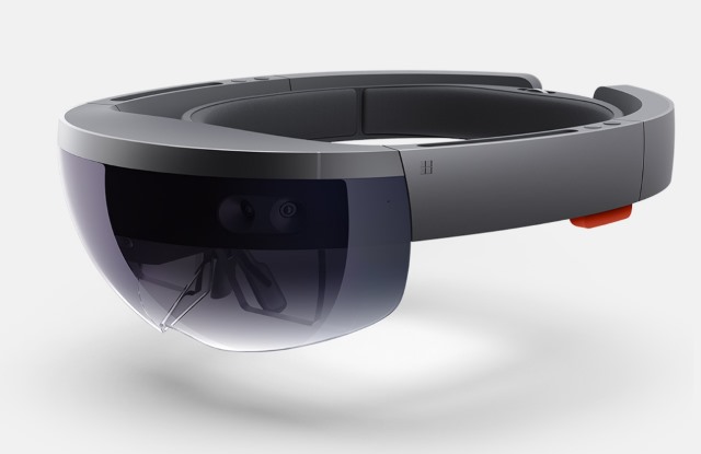
At the Hot Chips conference this week, Microsoft has shed some light on the hitherto secretive specifications of its augmented reality HoloLens. Now that anyone with $3,000 spare is able to buy a headset, there's never been more interest in what's actually inside the case powering the AR goodness.
The holographic processing unit (HPU) at the heart of HoloLens is a seriously multi-cored beast. The Register reports that it is a "TSMC-fabricated 28nm coprocessor that has 24 Tensilica DSP cores". Of course, there's much more to the device than just this chip.
The HPU is capable of processing a trillion calculations a second, with each core focusing on a specific task. This is all helped by 8MB of SRAM and 1GB of low-power DDR3 RAM. In addition to the HPU, there's also a 14nm Intel Atom x86 Cherry Trail SoC, packing 1GB of RAM and running Windows 10.
All told, HoloLens' HPU sucks under 10W of power, something which was made possible by using Tensilica's instruction extensions to add custom instructions to the DSPs. These algorithms, says Microsoft, are up to 200 times faster than if they were handled solely by software.