IBM Also Reinvents the Transistor
On the very same day that Intel announced to the world it had developed the critical formula for the material that will replace silicon dioxide as the dielectric gate in transistors for metal oxide semiconductors, its biggest arch-rival in the research and development field, IBM, announced the very same thing.
The still secret material, for years considered the "Holy Grail of semiconductor science," will enable transistors to scale down to the seemingly impossible levels Intel requires to feed the monster that is Moore's Law.
As the senior manager of IBM's T.J. Watson Research Center, Mukesh Khare, told BetaNews this afternoon, it too settled upon a hafnium based compound to replace SiO2. In empowering the first wave of high-k, metal gate (HK+MG) semiconductors, this new material, Khare said, will enable IBM and partners including AMD to leap over a critical stumbling block these engineers encountered when scaling their designs down past the 90 nm mark.
 "Historically, the industry had stopped thinning down the gate dielectric at 90 nm because of the leakage current increase," Khare told BetaNews, "because the gate dielectric thickness is seen as 11-12 angstroms [ten billionths of a meter]. You can imagine that's extremely thin, like two to three monolayers of SiO2." In other words, for the IBM processes used by AMD and the STI coalition (Cell processing engine), scaling down to 65 nm - where Intel is today - was proving to be problematic.
Scaling a semiconductor's size down takes place in two dimensions, both lateral - representing the typical layout - and vertical, which takes its cross section into account. At lower than three monolayers - three layers of molecules packed most closely together - the capacitance properties of SiO2 disappear, and the transistor leaks current.
"High-k stands for higher dielectric constant, where 'k' is the constant," Khare explained. "Once you have a higher dielectric constant material, you can use a physically thicker film for the same effective capacitance, because the way you control the charge in the transistor depends on the coupling or the gate capacitance. And that is good because ideally you want a high capacitance but lower leakage current. The two of them don't go hand-in-hand."

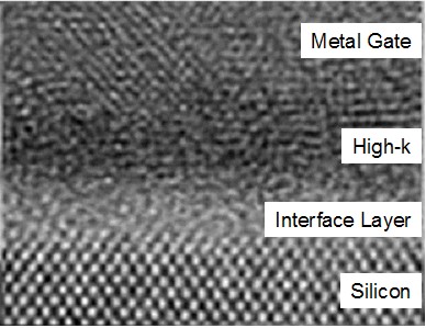
IBM's own HK+MG transistor, here seen in a cross-section electron microscope scan. (Courtesy IBM)
In other words, the hafnium compound fits the scale of transistors that are half the size for 45 nm processors that they are for 65 nm processors, and can hold their electric field more reliably, though the hafnium-based gates actually don't have to be scaled down to that three-monolayer level.
"If you know the transistor scaling concept, when you shrink the lateral dimension...you also have to scale the vertical dimension," stated Khare. "Since the SiO2 vertical dimension could not be scaled further, the lateral dimension shrinking also stopped, or slowed down quite dramatically. That's why it was very necessary for the industry to find an alternative to restart the scaling."
He added that as semiconductor designs became smaller, channel lengths had to be reduced proportionately. And that only exacerbated the gate dielectric problem: "When you scale a channel length, you have to also scale the gate dielectric thickness in order to keep the same electric field."
Perhaps with a little more historical perspective over time, we could learn this was the stumbling block that put AMD behind Intel on the lithographic scale by one generation: Their 65 nm generations could become smaller from the "top view," but not from the "cross section." More evidence may yet be revealed.
There is still quite a bit of information about IBM's research that we still don't know at present, and that Khare was not at liberty to reveal. The identity of the metal being used as the electrode, to substitute for polysilicon, remains a mystery today, though he said IBM is preparing to reveal its identity at a future conference. The only clues to that formula come from documents posted to IBM's Web site prior to its HK+MG announcement, mentioning two candidates: titanium nitride (TiN) and tantalum nitride (TaN).
Khare also declined to state whether IBM had produced any working processors using the new compound, though he did say the process the research team has worked out is currently being integrated into a 300 mm production line. "Nothing is complete until it's really complete," he said, "so just before the volume production, that's when we really complete all the testing for quality, yield, and reliability."
Last Friday, Intel told reporters its laboratory engineers had actually produced working 45 nm HK+MG processors, and had tested them in laboratories running Windows Vista, Mac OS X, and Linux. They showed a picture of lab engineers toasting themselves with champagne to prove it.
Finally, IBM's Khare added a surprising note of uncertainty about whether the manufacturing process being worked out, once it's "really complete," can or will be adopted by AMD in time to meet its stated commitment of ramping up 65 nm production this year, and 45 nm production next year.
"IBM's partners are a part of this development, in both research and development, and they are up to speed and know exactly what the processes are," he stated. "After that, it'll be a choice of the companies to do it as they wish."