Intel Reinvents the Transistor
In a presentation to exclusively invited reporters Friday morning, Intel announced a breakthrough development in microprocessor manufacturing that may be given historical significance in decades to come: the discovery of a new molecular compound material that will replace silicon dioxide in microprocessors using 45-nm and smaller lithographies.
It is what both wide-eyed engineers and anxious executives have described as the "Holy Grail of semiconductor technology," and Friday morning Intel revealed it has developed working 45-nm processor samples running Microsoft Windows Vista, Mac OS X, Linux and other operating systems, where this material - a compound based on the element hafnium, atomic number 72, a frequently occurring impurity in zirconium typically found in fake diamonds - serves as the dielectric gate between the current source and the current drain.
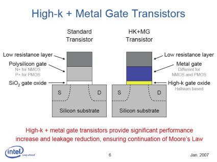
With the hafnium material serving as the gate, Intel will then replace the polysilicon electrode layer with a metal electrode, the exact alloy used here also being kept secret. As a result, transistors for 45 nm semiconductors starting with Intel's Penryn family will be fabricated at half the size of those used in today's 65 nm Core 2 processors. At the same time, transistor switching power can be reduced by as much as 30%, while still obtaining a performance improvement of as much as 20%. And current leakage at the gate will be reduced by a factor of 10.
How big of a page has been turned here, really? Since Intel announces advancements several times a year any more, what makes this one substantive beyond the typical hyperboles reserved for press releases?
Intel's current processor roadmap leaps between processor technology families every two years. We saw the latest leap just last summer, from the last of the Pentium D dual-core processors at 90-nm, to the Conroe/Merom/Woodcrest series at 65-nm. But while this "high-k + metal gate" (HK+MG) development does play into Intel's planned leap to the Penryn architecture, Friday's revelation literally marks only the start of a second era in metal oxide semiconductor production.

A diagram depicting the differences between a first-generation MOS transistor and an HK+MG transistor to be used in Intel's Penryn 45 nm CPUs. (Courtesy Intel)
Since the 1960s, gates have been made using silicon dioxide (SiO2), and electrodes have been made with polysilicon. Substrates are the third major material; historically Intel has used silicon or silicon germanium (SiGe), and the industry has experimented with gallium arsenide. HK+MG replaces two of the three compounds used in semiconductor transistors since the 1960s.
"These are not laboratory devices," Intel's director of process architecture and integration, Mark Bohr, announced Friday morning. "These are not just research results. We've actually made these transistors in a fully-integrated 45-nm CMOS process flow. We have high-K metal gate PMOS transistors [positive flow] and NMOS transistors [negative flow], both providing higher performance than the previous generation and lower leakage than the previous generation. This integrated process flow also meets our reliability requirements and is manufacturable in high volume."
It may not be a feat that goes unanswered by Intel's chief competitor. Last month, AMD, along with manufacturing partner IBM, announced at a materials conference the discovery of an ultra-low-k dielectric compound that those companies will use in the development of new interconnects in processors at 65-nm and lower lithographies.
"I don't want to underestimate the feat that these companies have achieved," Jim McGregor, principal analyst at In-Stat, told BetaNews. But HK+MG replacing the silicon gate with metal, he said, "is very, very significant because there's been significant issues with some of the early high-k [materials], in terms of the crystalline structure deterioration, as well as the fact that they're dealing with different types of materials, trying to bond them together [and] work together for a very long time with very high performance."
45-nm is the transition point, McGregor believes, where semiconductor manufacturers must change the materials and processes they've been accustomed to, simply because the same old materials don't behave the same way once they're so small. As Intel explained, as a transistor is made smaller, its gate dielectric layer naturally becomes thinner. Toward 65-nm, this hasn't been a bad thing; the thinner gate has led to an increase in the gate field effect, which is desirable. But over time, after everyday use, a depletion area emerges between the gate and the electrode, in effect thickening the gate area, increasing the level of current necessary to implement a switch, and degrading the overall "on" current.
Replacing silicon dioxide with the hafnium compound lets Intel go ahead and thicken the gate layer, which in turn naturally increases the amount of "on" current. Meanwhile, the replacement of polysilicon with a metal electrode completely eliminates the depletion of electrode area over time.
The "k" in the term "high-k dielectrics" refers to a material's relative ability to hold an electric charge. In electrodynamics, it's actually written with the Greek lower-case letter kappa. The "kappa," if you will, of silicon dioxide is about 3.9. That number means nothing until you compare it to that of hafnium compounds. Intel has not revealed whether the compound it discovered is based on hafnium silicate or hafnium oxide. The "kappa" for pure hafnium silicates has been observed in a range between 15 and 25, while pure hafnium oxides have been observed at 40. Intel is likely using an "impure" compound for the sake of structural integrity; laboratory tests on hafnium oxides yielded observed "kappa" of over 16. So it's quite possible that Intel's new compound may be as much as four times more efficient than silicon dioxide at holding a charge.
Next: Why Intel's enthused about high-k and AMD about low-k